
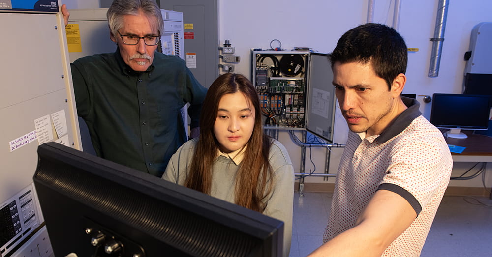
IEC Equipment
The IEC laboratories have a vast array of equipment – often custom- designed and built – to further our studies fulfill requests on behalf of our partners. Below is a list of current equipment being used in the IEC labs. Our equipment list changes constantly, and new pieces are added depending on project requirements.
Thin Film Deposition
- Vapor transport deposition system for depositing II-VI compounds onto moving 10×10 cm substrates in inert or reactive ambient over wide range of pressure and temperature.
- Three-source evaporator for depositing II-VI compounds and alloys.
- Six-chamber, in-line, plasma enhanced chemical vapor deposition for depositing a-Si:H and related alloy films and devices up to 30 × 30 cm area.
- Roll-to-Roll inline deposition system with four elemental effusion sources and in-situ flux control for depositing Cu(InGa)Se2 thin films onto a 15 cm wide moving web.
- Multi-source elemental evaporators for depositing Cu(InGa)Se2 and related alloys onto an array of nine 2.5×2.5 cm substrates.
- CVD reactor for steady state or RTP reaction of Cu/In/Ga or other layers with H2Se and/or H2S gas.
- Close space vapor transport system for perovskite film deposition integrated to glove system with controlled atmosphere.
- Close space vapor transport reactor for treating films in halide vapors.
- Chemical bath (CBD) and chemical surface (CSD) deposition of uniform CdS, ZnS and Cd1-xZnxS alloy films from 10 to 100nm thick.
- Electron beam evaporator with rotatable 4-source turret for depositing most metals and anti-reflection coatings.
- Electron beam evaporator with rotatable 4-source turret and two sputtering sources.
- Three target RF/DC sputtering system for deposition of ZnO, ITO, and other materials.
- Four target DC magnetron sputtering system for deposition of Cu, In, Ga, Mo, and other metals.
- Crest Ultrasonic substrate cleaning and drying facility.
- Assorted tube furnaces and drying ovens for heat treatment and reaction in air, argon, nitrogen, hydrogen, oxygen, and hydrogen-argon.
- Full positive & negative photolithography capability including spin coater, Suss Mask Aligner, and well-established etching procedures.
- Circulating de-ionized water facility with 11 stations and one Barnstead NanoPure water station.
PV Systems and Grid Integration
- 30 kVA 3-phase grid emulator that can mimic the electric grid conditions, including voltage amplitude, frequency, and phase angle.
- 5 kW Programmable PV simulators to drive DC power to the inverters that can control the I-V curve and solar irradiance profile.
- 3.8 kW residential grid-tied smart inverters with grid-supporting functions.
- A 4-channel power meter that can measure parameters from inverters, PV power supplies, and the grid emulator.
- Centralized equipment control from Chroma computer with remote communication and control through GPIB and Modbus protocols.
- 5 kW south-facing bifacial PV array with module Level Power Electronics (MLPE) and interchangeable ground reflectivity for albedo study.
- Temperature and irradiance sensors on representative modules to gather measurements from both front and rear sides.
- 3.8 kW DC-coupled grid-tied smart inverter with grid-supporting functions and energy storage control.
- 10 kWh Li-Ion battery that can control charging-discharging profiles
- Level 2 one-directional EV charging station.
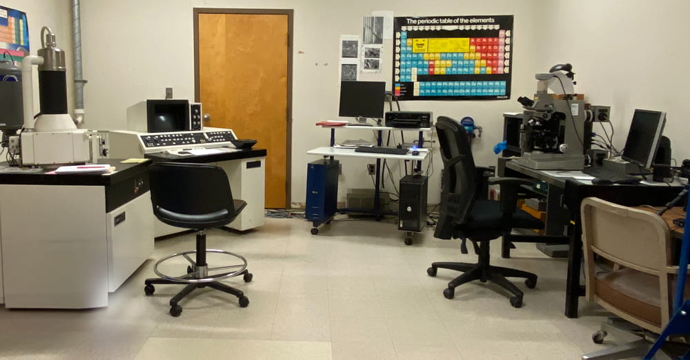
Material Characterization
- Amray 1810T Digital Scanning Electron Microscope (15X to 100,000X) with Energy Dispersive Spectroscopy (EDS) and Electron Back-Scatter Imaging capabilities.
- Olympus Optical Microscope with reflected, transmitted, and polarized illumination. Accessories include Nomarski optics and dual axis stage with verniers.
- Oxford Instruments X-strata X-ray fluorescence spectrometer
- Philips/Norelco Scanning Wide Angle X-ray Diffractometer with diffracted beam monochromation (CuKa) and digital control/acquisition.
- Philips Scanning Wide Angle X-ray Diffractometer with diffracted beam monochromation (CuKa, CrKa, CoKa), variable slits and digital control/acquisition.
- Rigaku D/Max Scanning X-ray Diffractometer with symmetric theta-2 theta and asymmetric glancing incidence geometries, variable slits, hot stage (to 450°C), and computer control/acquisition.
- PAR computer controlled Potentiostat-Galvanostat.
- Woollam Variable Angle Spectroscopic Ellipsometer.
- Perkin-Elmer Lambda-750 UV-visible-IR Spectrophotometer fitted with integrating sphere.
- ThermoScientific DXR Raman microscope.
- ThermoScientific Nicolet 6700 FTIR.
- Light and dark conductivity as a function of illumination intensity and temperature.
- Hall effect measurement system.
- Sinton lifetime and suns-VOC testing facility.
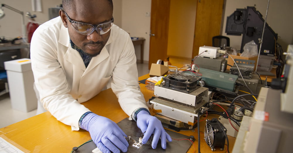
Device Analysis
- Current-voltage testing as a function of illumination intensity, spectral content, and temperature.
- Two Oriel Xenon solar simulators (AM1.5 global spectra).
- Spectral response with light and voltage bias capabilities.
- HP4274 and Hioki IM3536 LCR meters for capacitance measurements as a function of voltage, frequency, and temperature.
- Laser scanning facility-optical beam induced current.
- US Laser two-wavelength (1064nm, 532nm) laser scriber.
- Four-pod accelerated stress exposure facility, allowing up to 16 samples to be independently monitored and maintained under different states of controlled atmosphere, illumination, electrical bias and temperature.
- Two-chamber accelerated stress exposure facility for up to 2ft × 2ft illuminated area in controlled temperature and humidity ambient.
- Photoluminescence (PL) and electroluminescence (EL) mapping
- Asymtek Mechanical scriber and High resolution ink jet printer.
- Sheet glass cutting facility.
- Metallurgical polishing facility.

A new solar array that incorporates bifacial solar modules (those that absorb the sun’s energy from the top side and the bottom side) was installed outside the Institute of Energy Conversion, offering new research capacity to students and other researchers.
State-of-the-Art Facilities
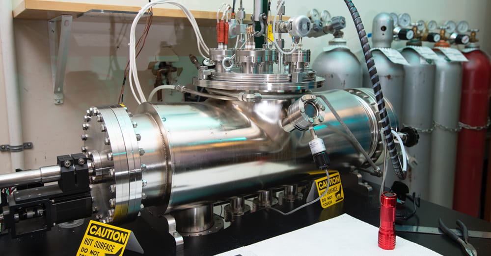
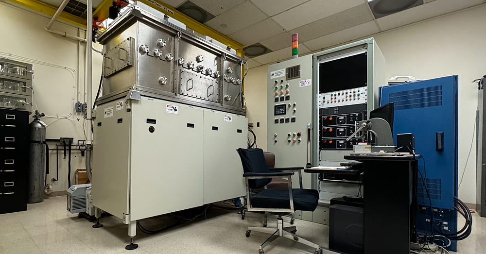
Vapor Transport System
Vapor-based deposition reactor for high throughput processing of CdTe thin film solar cells. Equipped with source for Group V dopant incorporation. The vapor transport reactor is used for deposition of cadmium telluride thin films to study novel ways to control the electronic properties of the materials.
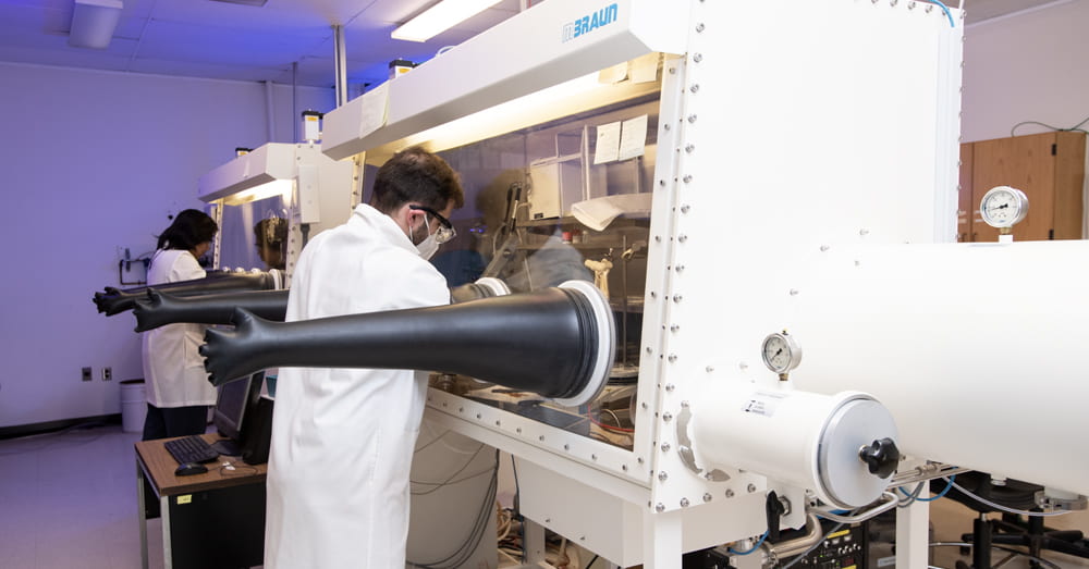
Perovskite Workstation
This is an In-house facility designed for vapor-processing of perovskite thin film, maintained in 2 gloveboxes allowing complete cell manufacture and measurement without exposure to air. This glovebox system is made by M-Braun.
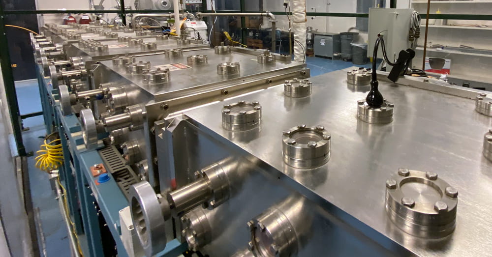
MC System
PECVD system for processing thin film layers in crystalline Si solar cell stacks. PECVD system for processing thin film layers in crystalline Si solar cell stacks using DC, RF or VHF power with in-situ monitoring of plasma characteristics.
Selenization
Unique research CVD reactors for safe and commercially-relevant manufacture of thin film CIGS solar cells through reaction of metal films with gaseous Se and S species.
HIL Lab
State-of-the-art laboratory designed for simulation of performance and resilience of smart energy grids.
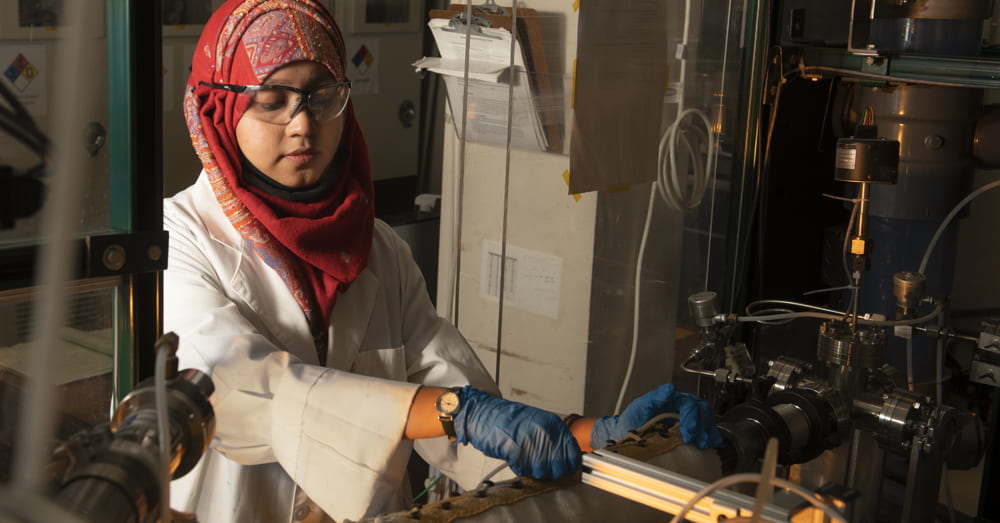
Materials Processing and Characterization
Many techniques available for thin film deposition and processing. These abilities are complemented by chemical, structural and optical-based materials characterization.
Solar Cell Characterization
Wide suite of device analysis and testing, including JV(T), spectral response, and accelerated cell stress exposure facility.
Roll-to-Roll Inline Deposition System on Flexible Substrate
Custom designed Roll-to-Roll deposition system with four elemental effusion sources and in-situ flux control for depositing CIGS thin films on moving flexible substrate.